

We have sufficient stock and also support customization. Flexible order quantity, if you only need few quantity we are your best choice . Sufficient stock with short delivery time, if you have urgent needed we are your best choice . Strong customization capability ,if your order with special specification we are your best choice .
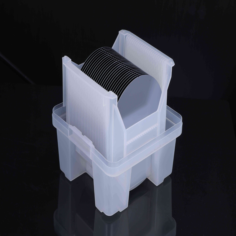
HC Wafer a silicon wafer supplier, we can offer FZ Silicon wafer, CZwafer, Test Wafer, Dummy Wafer, polished wafer, etching wafer.
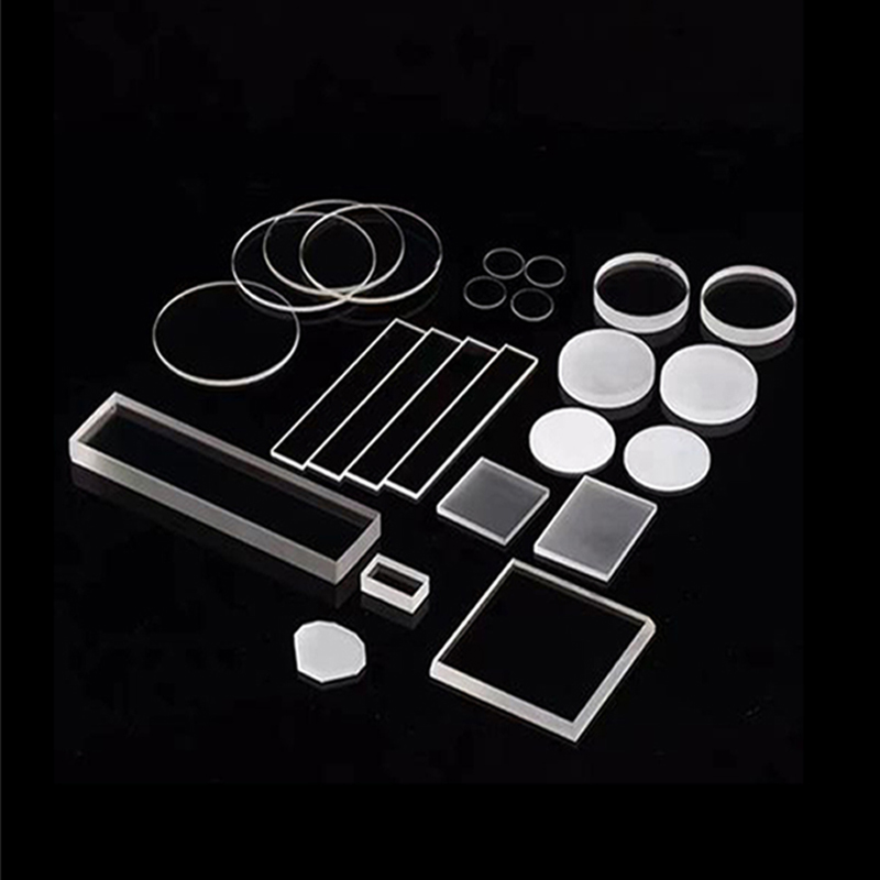
We can offer 2inch ,3inch,4inch,6inch sic substrate .Silicon carbide (SiC) is a novel compound semiconductor material with superior performance. Silicon carbide semiconductors have excellent characteristics such as large bandgap width (about 3 times that of silicon), high critical field strength (about 10 times that of silicon), and high thermal conductivity (about 3 times that of silicon). They are ideal semiconductor materials for making high-temperature, high-frequency, and high-power power electronic devices (power chips).
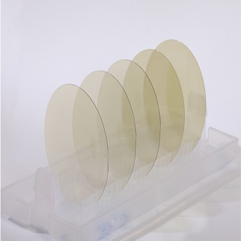
Hc wafer supply Ge germanium wafers. Size: 2-6 inches, other sizes can be customized. Crystal orientation: 100/111, off 4 °, 6 °, 9 °, etc. Conductive type: N-type, P-type, Undoped high resistivity .
Why Choose HC Wafer As Your
Reliable Choice For Semicon Wafer Supplier

We have sufficient stock of various products .The short delivery time and flexible order quantity.Send me your detail specification we will help find our stock for you .

If your specification is special we support customization with good quality .We will provide test report for keep all your specification request .

All our products will meet your specification request .We will provide test report before the shipment .

All our products with very good price .Welcome to your inquiry .

 Sep 28,2023
Subscribe And Save Stay in touch.
Subscribe to get notified about product launches, special offers and news.Address :Room 803, No. 44, Yindou Nanli, Jimei District, Xiamen, China


Copyright 2024@ HC Wafer Semiconductor Material. All Rights Reserved.Sitemap | blog | Xml | Privacy Policy  Network Supported