
Products


Silicon carbide is a third-generation semiconductor material with excellent physical properties such as high energy gap, high thermal conductivity, and high electron saturation drift rate. It has broad application prospects in high-temperature, high-power, high-pressure, high-frequency and other fields, such as electric vehicles, communication, energy, industry, etc.
Item No :
011Order(MOQ) :
1Payment :
100%PrepayProduct Origin :
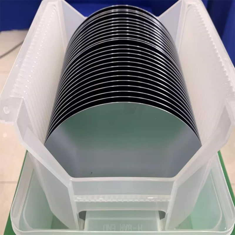
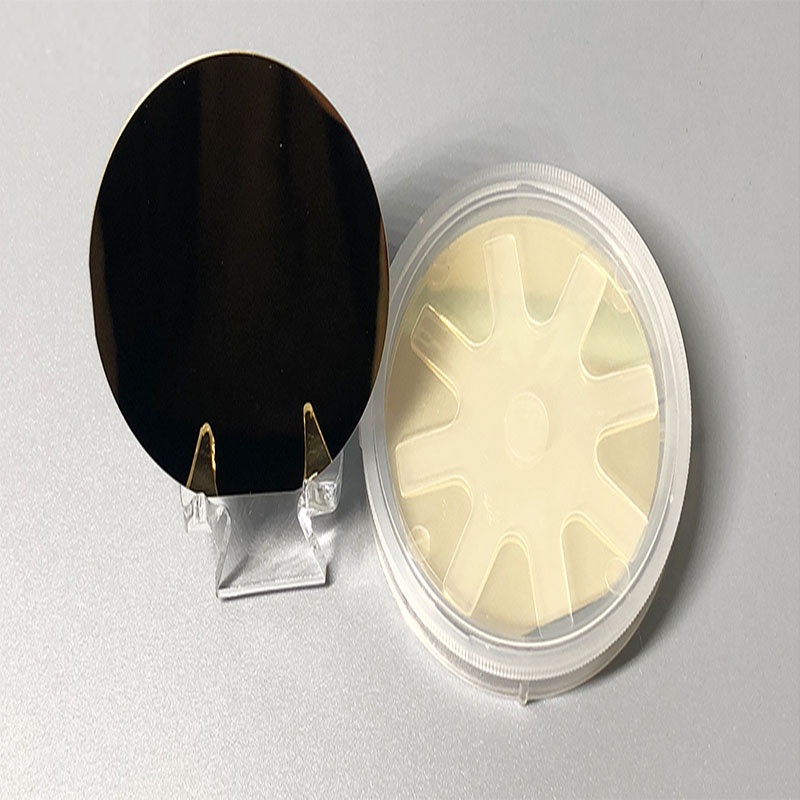
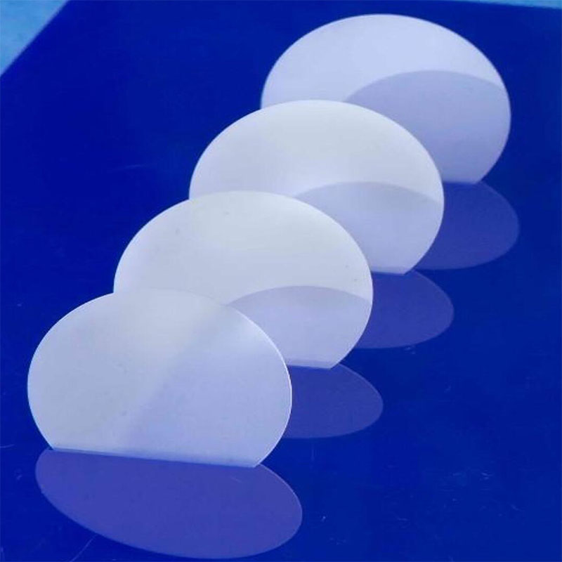
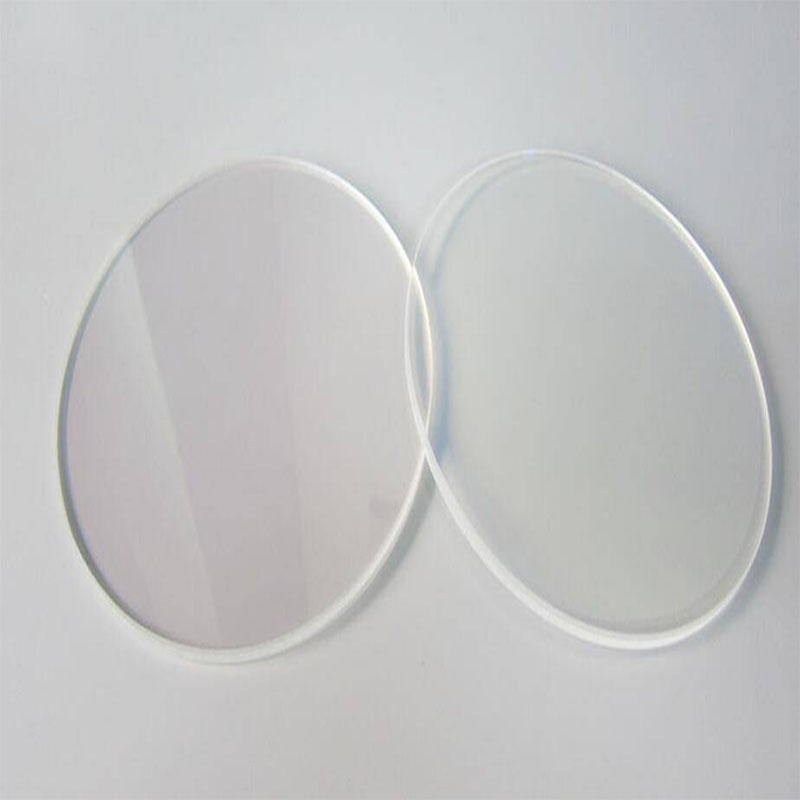
ChinaSilicon Carbide Substrate Wafer
| Polytype | 4H -SiC | 6H- SiC |
| Diameter | 2 inch | 3 inch | 4 inch | 6inch | 2 inch | 3 inch | 4 inch | 6inch |
| Thickness | 330±25μm | 330±25μm |
| Conductivity | N – type / Semi-insulating | N – type / Semi-insulating |
| Orientation | On axis <0001> | On axis <0001> |
| Off axis <0001> off 4° | Off axis <0001> off 4° | |
| Resistivity | 0.015 ~ 0.03 ohm-cm | 0.02 ~ 0.1 ohm-cm |
| (4H-N) | (6H-N) | |
| Micropipe Density(MPD) | ≤10/cm2 ~ ≤1/cm2 | ≤10/cm2 ~ ≤1/cm2 |
| TTV | ≤ 15 μm | ≤ 15 μm |
| Bow / Warp | ≤25 μm | ≤25 μm |
| Surface | DSP/SSP | DSP/SSP |
| Grade | Production / Research grade | Production / Research grade |
| Lattice parameter | a=3.076A , c=10.053A | a=3.073A , c=15.117A |
| Eg/eV(Band-gap) | 3.27 eV | 3.02 eV |
| ε(Dielectric Constant) | 9.6 | 9.66 |
| Refraction Index | n0 =2.719 ne =2.777 | n0 =2.707 , ne =2.755 |
| Note:We can provide customized .Welcome to contact us . |
|
|
Application:
1,Power electronic devices: Silicon carbide wafers have the ability to withstand high voltage and work at high temperatures, making them widely used in the field of power electronic devices.
2,Optoelectronic devices: Silicon carbide chips can be made into high brightness LEDs (light emitting diodes) for use in fields such as lighting, display, and communication. In addition, silicon carbide wafers can also be used to manufacture solar cells, with high photoelectric conversion efficiency and longer lifespan.
3,Infrared detectors: Silicon carbide wafers have high sensitivity to infrared radiation, making them widely used in the field of red detectors.
4,Automotive Electronics:The high-temperature working ability and high pressure resistance of silicon carbide wafers make them an ideal material in the automotive electronics field.
FAQ:
1:What's the minimum order quantity ?
We have stock so please inform the quantity you need and then we will check the quantity of our stock .If we don't have stock will base on our material we have .
2:What's the production time?
If we have stock the lead time around 2-3week .If need make production the lead time need discuss base on your quantity .
3:What is your payment method ?
Usualy by TT if you need other method pls discuss with us .
Subscribe And Save Stay in touch.
Subscribe to get notified about product launches, special offers and news.Address :Room 803, No. 44, Yindou Nanli, Jimei District, Xiamen, China


Link:
Network Card
Nbsmti
huaqingcn
amorphousoem
Reflectop
Copyright 2026@ HC Wafer Semiconductor Material. All Rights Reserved.Sitemap | blog | Xml | Privacy Policy  Network Supported